Samsung’s archrival wants to spread 100 special CPUs in every SSD controller ahead of PCIe 8.0, High Bandwidth Flash onslaught
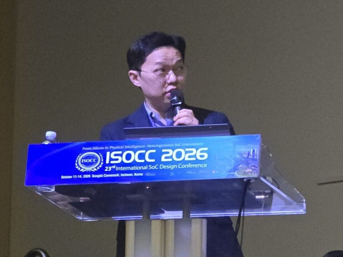
SK Hynix plans to distribute more than 100 processors across SSD controllers H-TPUs reportedly consume just 2. 5% of conventional CPU core power Each H-TPU occupies only 4% of a general-purpose processor core’s area SK Hynix is developing solid-state drive controllers with more than 100 compact processors to manage increasingly demanding data transfers. The South Korean memory manufacturer says its Hynix Transaction Processing Unit (H-TPU) architecture reduces processor power requirements and chip area. The technology is designed for enterprise storage products and future memory systems serving demanding artificial intelligence workloads. Small processors take over repetitive SSD operations Speaking at the recent International SoC Design Conference, SK Hynix vice president Koo In-je described limitations affecting conventional SSD controller designs. "Currently, general-purpose CPUs inside SSD controllers are at their limits in terms of power consumption and area," he said. "Instead, SK Hynix has developed an H-TPU that can efficiently handle common input/output (I/O) transmission paths." Conventional processors handle routine operations alongside demanding tasks, including reading and writing data, updating metadata, and controlling buffers. Faster storage interfaces increase these workloads, potentially requiring additional processor cores and increasing the controller’s physical footprint and electricity consumption. H-TPUs separate repetitive operations from complicated processing, allowing numerous specialized cores to handle individual responsibilities. SK Hynix says each processor uses just 4% of the chip area occupied by a general-purpose CPU core and consumes approximately 2. 5% of its power…